 PCB Solder Masking
Digital inkjet printing for applying solder mask on PCB boards has many significant benefits. That is why PCB manufacturers and material suppliers are transitioning towards direct printed solder mask.
Simplified Process Flow
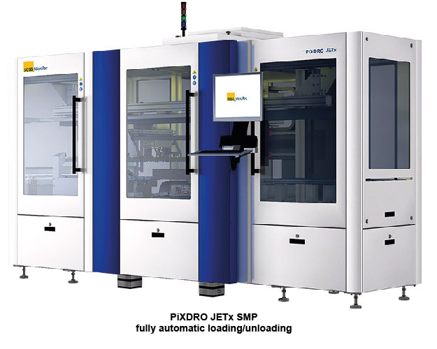
Compared to the traditional solder mask process, the number of process steps is reduced to three in the inkjet-based process. Pre-treatment remains crucial for good adhesion. The inkjet printer then applies the solder mask material and uses UV curing so the boards come out tack-free. Post-curing concludes the process. This simplification saves capital equipment, labor, process chemicals and waste, and reduces handling and the buildup of yield problems. It also cuts the total time to finish a PCB board – a key point in today’s fast-moving electronics business.
ADVANTAGES
 It is a selective coating technology: material is only deposited where required. This reduces material consumption and avoids the challenge of removing surplus solder mask material
- No risk of removing small solder dams between IC contacts
- Inkjet allows different surface finishes, layer thicknesses and materials. Finally, inkjet has the ability to accurately align and scale the print image to the board
- Inkjet has the ability to accurately align and scale the print image to the board
- Additive and cost-effective solder mask deposition, eliminating photo processes
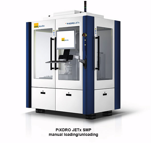
MACHINE FEATURES
- Alignment accuracy: <2 µm using automated fiducial alignment
- Layer thickness: 30-80 µm, can be varied over the board to reduce material consumption
- >10 µm solder mask thickness on copper
- Solder mask openings: down to 100 µm
- Edge roughness: 20 µm
- Line-space: 75-75 µm
All information subjected to change without notice!
For more information, visit the website or send us your information request.


