 Direct Imaging System
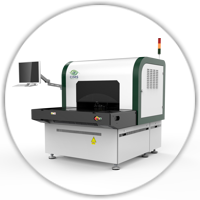
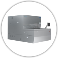
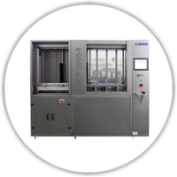
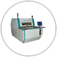
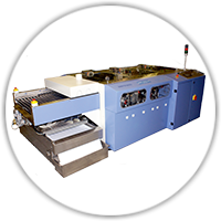
Ucamco has partnered with Dainippon Screen to introduce Ledia 5, Screen's revolutionary Direct Imaging machine to the European market. Ledia Direct UV-LED Imaging offers unparalleled benefits over traditional laser direct imaging.
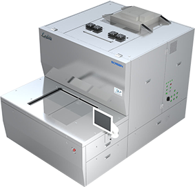 Ledia incorporates a UV-LED light source with broad wavelength spectrum resulting in:
- Optimal imaging of a wide range of solder mask and resist film type
- Optimal curing over the whole depth of the solder mask and resist film
- Imaging of conventional solder mask film with high throughput
- Imaging of conventional resist film with high throughput
- Low operational costUp to 5 times faster than current systems
3 Simultaneous wavelengths
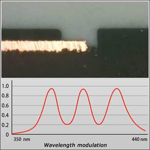 Ledia’s unique UV-LEDs light source combines two or three different wavelengths simul-taneously. The wave-length ranges from 350nm to 440nm to diffuse the energy optimally throughout the resist or solder mask. The user can tune each wavelengt’s power individually for optimal results on or each material. The result is high throughput and unrivalled quality – 50µm solder mask dams without undercut.
Drop-in
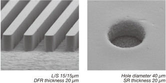 Ultra-fine feature capabilities, a precision auto-focus and an automatic alignment algorithm compensates for substrate distortion. Ledia exposes a wide range of both dry film and Soldermask with high-throughput and high-yield. As Ledia delivers top quality even on conventional resists it integrated into existing production environments with minimal hassle by Ucamco’s experienced hardware and software installation team.
MODELS
Our Direct Imaging Systems are available in various panel size capability models to best suit our customer's imaging production needs.
All models share the same basic qualities:
- Straightforward and robust 'maintenance free' design
- Seamless integration with existing CAM system
- Fully configurable = drop-in system to replace or complement existing direct imaging system
- The Ledia available in 3, 5 & 6-Head configuration
- Field Upgradeability possible
ADVANTAGES
- Latest UV-LED Technology
- Latest DMD Technology (Digital Mirror Device)
- Direct Optical Path to Substrate
- Autofocus following surface topography of PCB
- Automation ready
- Lowest Cost of Operation
- Long & Reliable LED Lifetime
- Ideal for Soldermask application due to patented multiple Wave Length System
- Exposes Soldermask equally on top and bottom with range between 350-420nm
- Pre-Programmable Wavelengths and Power
- Suitable for all Standard Resists and Standard Soldermask Inks
MACHINE FEATURES
- Size and Weight with Automation: W3200mm x D2900mm x H2100mm
- 30µm line/space (optional 10/15/20µm possible)
- Max. Panelsize: 540 x 661mm
- Positional Accuracy: 10µm
- Minimum Line/Space: 2,5µm
- Throughput:
- 7mj = 240 Sides p/hr
- 40mj = 180 Sides p/hr
- 240mj = 59 Sides p/hr
- Local Alignment in „Real Time"
- Calibration- and Alignment camera both controlled by High Precision Glass Scale
- Automatic data Integrity Check
- Input Formats: Gerber, DPF, ODB++
- DI Software Management Software for Batch Processing and Automatic Exposure
- Lower Energy Consumption than LDI
- Vacuum- and Clamping system also for thicker panels
All information subject to change without notice!
For more information, visit the website or send us your information request.


