Slide background
Slide background
Slide background

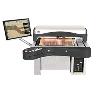
VVR for ICS

CIMS 2 2018AOI verification station for IC Substrates with min line/space down to 4 µm.

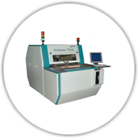
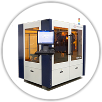
VVR, CIMS verification station combines virtual and physical verification within a single workstation. VVR for ICS is designed to support high volume manufacturing of IC Substrates. The systems within this series include the following models:

• VVR 4μ is optimized for verification of 4 µm line/space width technology
• VVR 5μ is optimized for verification of 5 µm line/space width technology
• VVR 7μ is optimized for verification of 7 µm line/space width technology
• VVR 10μ is optimized for verification of 10 µm line/space width technology
• VVR 15μ is optimized for verification of 15 µm line/space width technology

In VVR mode, operator starts by reviewing defects’ images grabbed by AOI and processed with AI-based image enhancement algorithms enabling quick filtering out obvious false calls. Using VVR enables dramatic improvement in verification efficiency and speed while seamlessly integrating the results with the database. Moreover, users can easily classify defects using an optional touchscreen providing a critical feedback to QA in real time.

VVR for ICS is compatible with all CIMS AOI.
VVR

 Highlights

  • Combines verification of AOI post-processed images with live video mode
  • Up to 70% increase in verification efficiency vs. traditional mode
  • Displaying post-processed color defects’ images grabbed directly from AOI
  • Variable zoom and automated calibration;
  • Stationary vacuum tables
  • Ergonomic design
  • Clear defect image and adjustable video light

 Options

  • Auto-marker for marking defects
  • Barcode reader
  • Adjustable monitor arm
  • CDB/CDBIC – defects classification and virtual defects mapping
  • SharpLight – enhanced video image


 All information subject to change without notice!


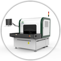
Galaxy 10x

CIMS 2 2018AOI for IC Substrates with min line/space down to 10 µm.

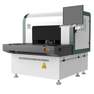
AOI for IC Substrates and ultra fine line HDI with min line/space down to 10 µm. Galaxy 10χ, CIMS latest generation of AOI system, is designed to support high volume manufacturing of IC Substrates and ultra fine line HDI. It is capable to scan down to 10 µm line/space width technology. The system’s state of the art optical technology Prisma Gen II™ is designed to provide flexible light coverage with maximum contrast in order to support high resolution image acquisition at high scanning speed. Optimized performance is achieved by combining sharp high resolution image with customizable detection algorithms. Equipped with the state-of-the-art image acquisition and advanced software capabilities, the Galaxy product family is renown for its exceptional detection achieved with lowest possible false calls rate.

Galaxy 10xGalaxy 10x is powered by Spark™ – an innovative cross-platform detection engine

 Highlights

  • Linear motors for smooth and silent motion
  • Compact mechanical platform
  • 6th Generation hardware
  • Enhanced illumination block 
  • Fast and intuitive setup for new jobs
  • Compatible with front AMHS automation or robot

 Options

  • Fi – final inspection option for finished boards
  • +2DM metrology – panel dimensions measurement
  • +2CD metrology – 2D measurement of circuit elements
  • +3DH metrology – 3D measurements of circuit element’s height
  • +3DP metrology – 3D profiling of circuit element
  • LDI – laser drill inspection option
  • CDB/CDBIC – defects classification and virtual defects mappingn
  • VVS – virtual verification system

microlight spark


All information subject to change without notice!


Galaxy 5x

CIMS 2 2018AOI for IC Substrates with min line/space down to 5 µm.

Galaxy 5χ, CIMS latest generation of AOI system, is designed to support high volume manufacturing of IC Substrates. It is capable to scan down to 5 µm line/space width technology. The system’s state of the art optical technology Prisma Gen II™ is designed to provide flexible light coverage with maximum contrast in order to support high resolution image acquisition at high scanning speed. Optimized performance is achieved by combining sharp high resolution image with customizable detection algorithms. Equipped with the state-of-the-art image acquisition and advanced software capabilities, the Galaxy product family is renown for its exceptional detection achieved with lowest possible false calls rate.

Galaxy 5xGalaxy 5x is powered by Spark™ – an innovative cross-platform detection engine

 Highlights

  • Linear motors for smooth and silent motion
  • Compact mechanical platform
  • 6th Generation hardware
  • Enhanced illumination block 
  • Fast and intuitive setup for new jobs
  • Compatible with front AMHS automation or robot

 Options

  • Fi – final inspection option for finished boards
  • +2DM metrology – panel dimensions measurement
  • +2CD metrology – 2D measurement of circuit elements
  • +3DH metrology – 3D measurements of circuit element’s height
  • +3DP metrology – 3D profiling of circuit element
  • LDI – laser drill inspection option
  • CDB/CDBIC – defects classification and virtual defects mappingn
  • VVS – virtual verification system

microlight spark


All information subject to change without notice!


Galaxy 7x

CIMS 2 2018AOI for IC Substrates with min line/space down to 7 µm.

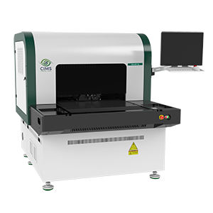
AOI for IC Substrates with min line/space down to 7 µm. Galaxy 7χ, CIMS latest generation of AOI system, is designed to support high volume manufacturing of IC Substrates. It is capable to scan down to 7 µm line/space width technology. The system’s state of the art optical technology Prisma Gen II™ is designed to provide flexible light coverage with maximum contrast in order to support high resolution image acquisition at high scanning speed. Optimized performance is achieved by combining sharp high resolution image with customizable detection algorithms. Equipped with the state-of-the-art image acquisition and advanced software capabilities, the Galaxy product family is renown for its exceptional detection achieved with lowest possible false calls rate.

Galaxy 7xGalaxy 7x is powered by Spark™ – an innovative cross-platform detection engine

 Highlights

  • Linear motors for smooth and silent motion
  • Compact mechanical platform
  • 6th Generation hardware
  • Enhanced illumination block 
  • Fast and intuitive setup for new jobs
  • Compatible with front AMHS automation or robot

 Options

  • Fi – final inspection option for finished boards
  • +2DM metrology – panel dimensions measurement
  • +2CD metrology – 2D measurement of circuit elements
  • +3DH metrology – 3D measurements of circuit element’s height
  • +3DP metrology – 3D profiling of circuit element
  • LDI – laser drill inspection option
  • CDB/CDBIC – defects classification and virtual defects mappingn
  • VVS – virtual verification system

microlight spark


All information subject to change without notice!
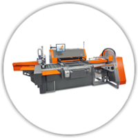
 

Galaxy 4x

CIMS 2 2018AOI for IC Substrates with min line/space down to 4 µm.

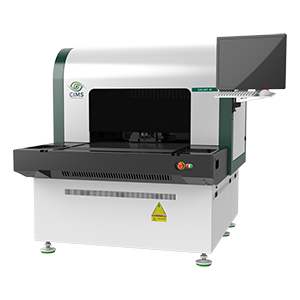
Galaxy 4χ, CIMS latest generation of AOI system, is designed to support high volume manufacturing of IC Substrates. It is capable to scan down to 4 µm line/space width technology. The system’s state of the art optical technology Prisma Gen II™ is designed to provide flexible light coverage with maximum contrast in order to support high resolution image acquisition at high scanning speed. Optimized performance is achieved by combining sharp high resolution image with customizable detection algorithms. Equipped with the state-of-the-art image acquisition and advanced software capabilities, the Galaxy product family is renown for its exceptional detection achieved with lowest possible false calls rate.

Galaxy 4xGalaxy 4x is powered by Spark™ – an innovative cross-platform detection engine

 Highlights

  • Linear motors for smooth and silent motion
  • Compact mechanical platform
  • 6th Generation hardware
  • Enhanced illumination block 
  • Next generation computer to process large data
  • Fast and intuitive setup for new jobs
  • Compatible with front AMHS automation or robot

 Options

  • Fi – final inspection option for finished boards
  • +2DM metrology – panel dimensions measurement
  • +2CD metrology – 2D measurement of circuit elements
  • +3DH metrology – 3D measurements of circuit element’s height
  • +3DP metrology – 3D profiling of circuit element
  • LDI – laser drill inspection option
  • CDB/CDBIC – defects classification and virtual defects mappingn
  • VVS – virtual verification system

microlight spark


All information subject to change without notice!
 

Information request

Please type your full name.
Invalid email address.
Please send us your message.
Invalid Input

About Adeon

At Adeon we believe that it is the quality of our work that placed us in our current position, and quality is what we try to improve with everything we do. European PCB manufacturers are often challenged to produce many different designs and technology levels every day. This makes it challenging to select and provide equipment that is capable of doing that. Our goal is to offer the best service and support against affordable rates to the highest standards to help our customers to stay at the forefront of technological developments.

Upcoming events

Contact

Weidehek 26
Industrial Area Haagse Beemden # 4530
NL-4824 AS Breda
The Netherlands
Telephone: +31 (0)76 541 00 08
Fax: +31 (0)76 542 50 59
E-mail: info@adeon.nl

More...