Slide background
Slide background
Slide background

ACB Group invests in new Flying Probe System

acbACB Group Invests in State of the Art Flying Probe Test System from ATG-LM:Atg LM Logo RGB White background

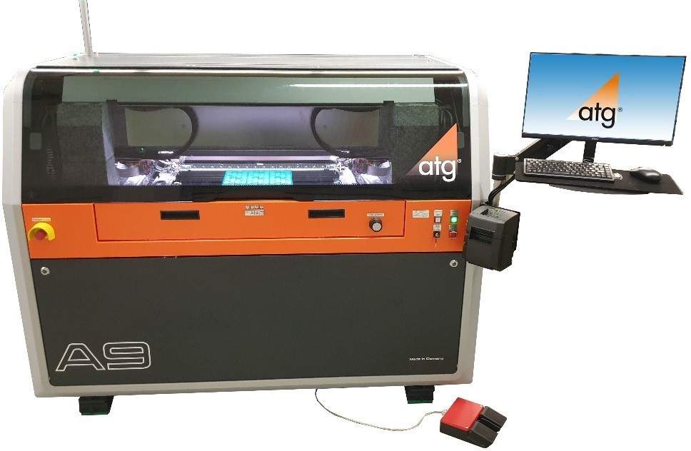
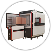
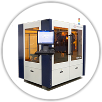
The ACB group is one of Europe’s largest independent manufacturers of highest technology printed circuit boards. The group consists of manufacturing facilities at Dendermonde (Belgium), Atlantec and Cibel (France)A9

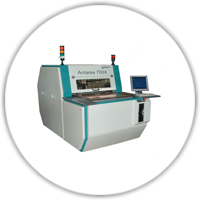
Following a comprehensive investment plan for the ACB Group, the group’s subsidiary Atlantec took delivery and installation of the brand new A9 system from atg-LM through its distributor ADEON Technologies. The ACB group has a long term experience with the Flying Probe Electrical test systems from atg-LM.

There is a clear increase of complexity throughout the range of Printed Circuits that are required by the end users. The demand for higher volume, as well as higher mix of products prescribe the need for reliable electrical test systems to secure the 100% functionality of the products. Additional fact is that the amount of circuits, and as a result the amount of testpoints, are increasing per design and the features to be tested are getting smaller all the time also.

It was therefore a rather obvious decision to purchase the state of the art new A9 system from atg-LM. The company are the world leaders by far in electrical flying probe testing of printed circuits. Besides the price to performance ratio atg-LM delivers reliability, robustness, speed, accuracy and a first class service through its distribution partner. The A9 systems are fully compatible with the other systems in use in the ACB group, but the speed and accuracy of the new system is unrivalled.

The increasing demand of supporting high-tech Printed Circuit Board manufacturing is recognised and supported also by the France Relance Project. The ACB group wishes to sincerely thank the « Loire Atlantique Préfet supporting French Electronics Manufacturing »

CCI Eurolam SA acquires Adeon Technologies BV

cci adeonParis (F) , Breda (NL) January 1 - 2021

CCI Eurolam Group, a leading distributor and industrial service provider to the EMEA electronics manufacturing industry, announced the signature of an agreement to acquire Adeon Technologies BV, a major full service provider of equipment for the European PCB Industry.

Alain Kahn, President of the CCI Eurolam group: “we are thrilled to welcome Adeon into the CCI Eurolam family. The current context shows a strong dynamics regarding manufacturing and we are excited to participate and support the favorable industrial investment trend in the EMEA region.”

Samuel Bismuth, Business Development Manager at CCI Eurolam Group commented: “There is a strong strategic fit between our companies and with the support of the CCI Eurolam Group, Adeon will keep strengthening its capabilities to expand and accelerate its growth. We believe that in the next decade, Equipments will be more than ever a strategic driver for technology in the electronics manufacturing industry and that Adeon is the right partner for the future.”

Andre Bodegom, Managing Director and owner of Adeon said, " At Adeon, we have been able to develop over the last 10 years a strong expertise in selling and servicing equipment over the EMEA region partnering with leading equipment manufacturers. As we started discussion with CCI Eurolam, it immediately became apparent that both healthy companies have a lot to offer to each other. The European PCB market is developing rapidly into various highly specialised companies, for which the combined expertise of CCI and Adeon will create a lot of Added Value. Becoming part of the strong and renowned CCI Group of companies will allow us to materialise our growth plans for the future in an even faster pace. Adeon will continue to operate from its base in Breda, The Netherlands in a business as usual manner."

MKS Sees Strong Early Market Adoption in Asia

MKS-ESI_Logo

for its Newest HDI PCB Laser Manufacturing Solution

Multi-system order for ESI® Geode system will enhance Meiko Electronics, Japan’s HDI PCB manufacturing capabilities

MKS Instruments, Inc. (NASDAQ: MKSI), a global provider of technologies that enable advanced processes and improve productivity, announced that Meiko Electronics Co. Japan has purchased multiple ESI® Geode™ systems to enhance its high-volume HDI PCB manufacturing capability. The recently released CO2-laser-based systems will be deployed at Meiko’s high-end manufacturing facility in Vietnam.

“We are pleased with the market adoption of the Geode system” said MKS President and CEO John T.C. Lee. “Geode is well-positioned to take advantage of the growing market for HDI PCB processing solutions, as electronics manufacturers continue the path of miniaturization in order to meet the demand for smaller and more capable devices.”

The Geode system delivers many benefits for high-end applications, such as 5G. According to Atsushi Sakate, Executive Officer, General Manager of Production at Meiko, “Beyond the Geode system’s higher drilling throughput and accuracy, the system’s smaller footprint and lighter weight enables us to plan capacity expansion with much more flexibility. Add to this the broad range of applications and materials that Geode can process, and the decision is clear.”

Developed by MKS’ Equipment & Solutions Division, already a market leader in flex PCB laser drilling solutions, the Geode system is optimized to process the rigid HDI PCBs and package substrates widely used in consumer electronics, such as smartphones and other handheld devices. Building on MKS’ technology leadership in laser processing for flexible printed circuits, Geode’s new CO2 laser technology and control capabilities deliver breakthrough performance. Its superior throughput, refined power control and small system footprint meet the needs of high-volume PCB manufacturers.


About MKS Instruments

MKS Instruments, Inc. is a global provider of instruments, systems, subsystems and process control solutions that measure, monitor, deliver, analyze, power and control critical parameters of advanced manufacturing processes to improve process performance and productivity for their customers. Their products are derived from MKS' core competencies in pressure measurement and control, flow measurement and control, gas and vapor delivery, gas composition analysis, electronic control technology, reactive gas generation and delivery, power generation and delivery, vacuum technology, lasers, photonics, optics, precision motion control, vibration control and laser-based manufacturing systems solutions. MKS also provides services relating to the maintenance and repair of their products, installation services and training. MKS' primary served markets include semiconductor, industrial technologies, life and health sciences, research and defense. Additional information can be found at www.mksinst.com.


About the ESI Brand

ESI® is a brand within the MKS Instruments Equipment & Solutions Division. The ESI portfolio consists of laser-based micro manufacturing systems and component test systems that are used worldwide by manufacturers in the electronics industry to process the materials and components that are an integral part of the electronic devices and systems in use today. Leveraging over 40 years of laser-material interaction expertise and applied laser technology, ESI solutions enable customers to optimize production by providing more control, greater application flexibility and more precise processing of a wide range of materials. The result is higher production quality, increased throughput and higher back-end yields at a lower total cost-of-ownership. Additional information can be found at www.esi.com.

Electro Scientific Industries and ESI are registered trademarks of MKS Instruments, Inc. All other trade names referenced are the service marks, trademarks or registered trademarks of their respective companies.


About Meiko

Meiko Electronics Co., Ltd. Japan, is a leader in the design, manufacture and sale of printed circuit boards and auxiliary electronics. Its PCB Business provides state-of-the-art products such as AnyLayer HDI—which enables connectivity between all layers—adapted to the shrinking size of mobile phones and other handheld devices. Meiko also provides high-heat-dissipation PCBs and high-electric-current PCBs capable of withstanding harsh environments, such as those found inside car engines and solar power generators.

 

geode composite


Exception PCB purchases Ledia Direct Imager

logoException PCB, one of the largest dedicated time and technology PCB manufacturers in the UK, has purchased a Ledia Direct Imager from Ucamco. To great satisfaction of all parties involved.
 More specifically, the direct imager is a Ledia 6 3-head 3-wavelength type. As the name suggests, the Ledia’s unique UV-LEDs light source combines three different wavelengths simultaneously. The wavelength ranges from 350nm to 440nm to diffuse the energy optimally throughout the resist or solder mask. The user can tune each wavelength’s power individually for optimal results on or each material. The result is high throughput and unrivalled quality – 50µm solder mask dams without undercut.

“The investment was part of our strategy to strengthen our advanced technical capabilities and to respond to the demands of our customers with faster quick turnaround (QTA) services”, Kamal Berberi explains. Exception PCB’s Operations Director lists his criteria in the search for a new direct imager: “Ledia 6 responds perfectly to our technical roadmap. It offers great capability on small fine lines and gaps, is highly accurate at solder mask registrations, and all this comes at a competitive price.” When asked about Exception’s early experiences with their Ledia, Berberi smiles broadly. “The transition from film to filmless solder mask was very smooth with Ledia. After two months, we have not encountered any issues whatsoever with our Ledia 6. We are now able to offer a quicker service to our customers, with absolutely perfect solder mask registration.”

The Ledia was purchased through ADEON Technologies from The Netherlands who are the Ucamco agents. André Bodegom comments: “We have a relationship with Exception PCB since 1993 as their supplier and service partner for various types of equipment. The relationship is based on providing the service that fits with Exception PCB’s requirements and we are truly proud to have been recognized as their Direct Imaging Supplier also, showing further growth even after all these years of working together. We have experienced from the technical staff at Exception PCB that they are very happy with the way the machine was installed, the training, the results and the services provided by Ucamco. The entire project fulfils us with pride.”

The same feeling is present at Ucamco, where Imaging Product Group Director Michel Van den heuvel is responsible for the hardware department. “The investment Exception PCB has done, is a great example of a company looking to optimize its services in an endeavor of continuing to boost performance”, he comments. “After the installation of the Ledia 6, we remain standby to provide technical and maintenance services. If the need should arise, we can be quickly on-site, thanks to our local network of highly skilled engineers and our local spare parts stock. Our Ledia’s uptime is unbeatable. We are confident Exception PCB will enjoy the benefits of their Ledia for a very long time.”

Ucamco releases Integr8tor v2020.08

Always a step Ahead!

I8 Flow

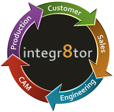
Today, Ucamco will release Integr8tor v2020.08. Below is a list of the most significant improvements.

  • UcamX Workflow Edition (WE) Graphics Editor
      • All-round workhorse addresses incoming data issues – no delays
  • Must-have additions to the QED Report for meticulously accurate quotations
      • Anomalies section to bring suspicious situations to your attention
      • Minimum BGA size to flag potentially critical component areas
      • Minimum solder mask opening detection for adequate process selection
      • Legend-to-pad clearance analysis for single-sided and maskless products
      • Summary section overhaul for an improved user experience
  • Stepping up the automation and speeding up the task
      • Automatic outline creation from corner marks – higher first-pass hit rate
      • Drill span recognition – automatic stackups for complex builds or any-layer HDI technology
      • RegionMaker and PadMaker – spot-on data optimization routines for a head start in CAM
      • Gerber Job File input automating the entry of PCB characteristics – hassle-free & rock-solid
      • Automatic zero-size aperture removal – another tedious task less for CAM
  • Cockpit Extensions
      • High Security option: restrict the viewing of sensitive jobs to your accredited staff only
      • New solder mask types and surface finishes

An elaborate explanation is available via https://www.youtube.com/watch?v=LQrsZxtDT-Y.


Ucamco 2019