Inkjet Printing Solution for High Volume Production
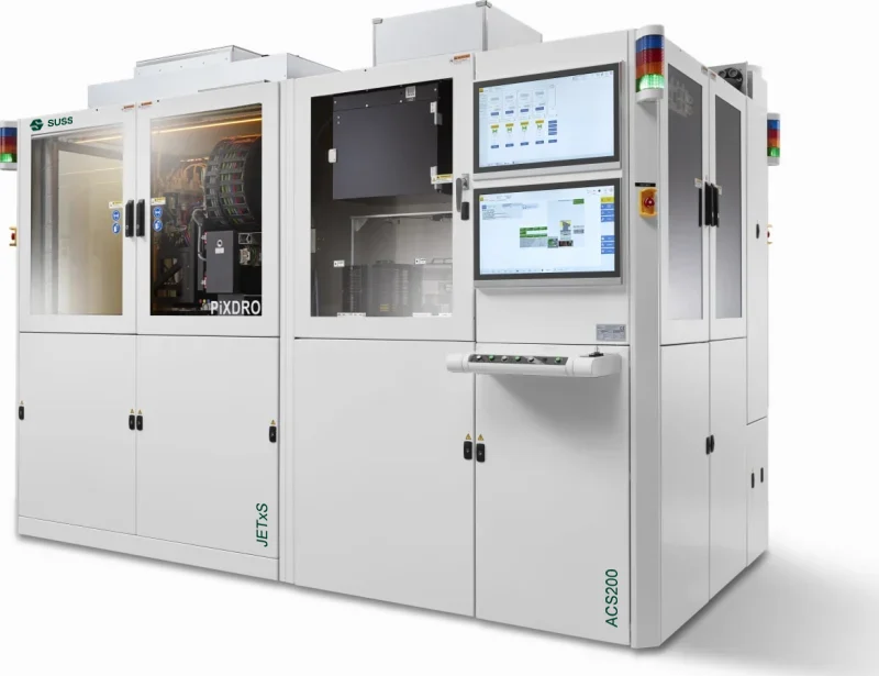 The JETx inkjet printer for high volume production is SUSS’s most advanced solution for printing functional materials, specifically designed for the semiconductor and adjacent markets, such as power electronics, sensors, MEMS, display and biomedical.
- The JETx, combined with a material handling unit, such as the ACS200 Gen3 TE, and a hotplate stack offers a complete production solution designed for a low cost of ownership with high throughput.
- Maximum substrate size: 610x762mm (24x30inch)
- Maximum substrate thickness: 10mm
- Substrate clamping: Vacuum Bed (optional mechanical assist)
- Base Frame: Granite
- Stage accuracy: ± 5µm (3s)
- Motion: Linear
- Print Speed: up to 1000mm/s
- Printhead Nozzles 128-2048 nozzles per head (2-80pL dropsize
- Data Formats: Gerber274X, DPF, ODB++, TIFF, postscript
- Footprint: 1200 x 2000 x 2000 (W, L, H)
- Weight: 1800kg
Highlights
- Green process
As an additive technology, inkjet printing is a green process compared to the traditional subtractive manufacturing techniques. Only printing the exact amount of material, exactly where it is needed, significantly reduces the amount of wasted material and eliminates removal-processing steps of excess material. - Fully integrated production solution
The JETx and ACS material handling unit offers a fully integrated production solution for direct patterning of materials such as photoresist, phase-change resist, dielectrics, such as polyimide, SU-8 and solder mask, but also conductive inks and customer-specific materials. - Optimized productivity, with low cost of ownership
One of the advantages of inkjet printing is that scaling up the productivity simply implies more printheads - Customizable configuration optimized for your process
JETx can be configured with multiple printheads and multiple ink systems to optimize the productivity. - Ink compatibility
Compatible with solvent-based, aqeous, hot-melt and UV curable inks - Pre- and Postprocessing Options
Within the ACS and JETx multiple pre- and postprocessing options are integrated, such as wafer pre-aligner with a barcode scanner, high-resolution camera for fiducial alignment, inline UV (Ultra-Violet) and NIR (Near Infra-Red) pinning/curing, hotplate and coolplate stack.
Main features and options
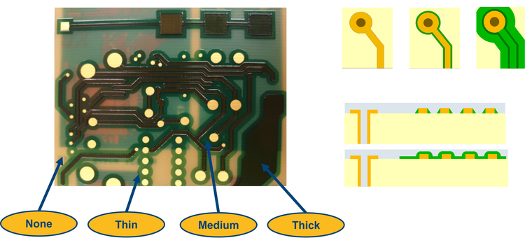 Full Control of Printing in selected areas and Thickness
- Advanced Drop Analysis (ADA) for best ink jetting performance
- Automatic Print Optimization (APO) for best application results
- Fully automated production solution
- Virtually zero material waste
- Minimal floorspace
- Individualization of products by digital processing
- Non-contact deposition for fragile substrates
- Micrometer control of layer thickness
- Integrated pre- and postprocessing options
- Continues operation during refill
- Automatic process inspection
- Easy to operate and maintain
Advanced PCB Distortion Correction
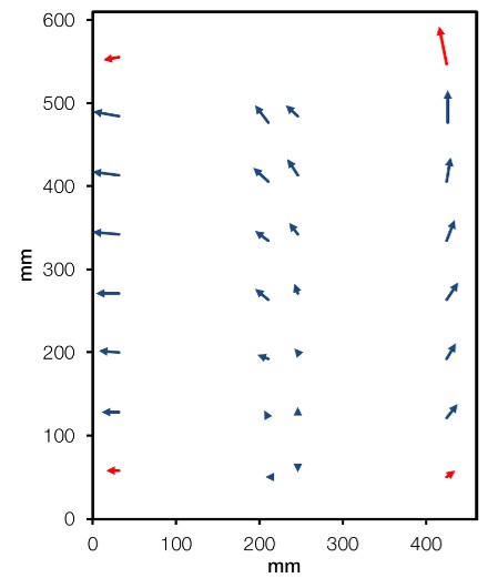 Digital printing enables PCB specific distortion corrections
- Perfect solder mask registration with multi-point fiducial
marks alignment - Local corrections for linear and higher order distortions
Advanced Production Flow Control
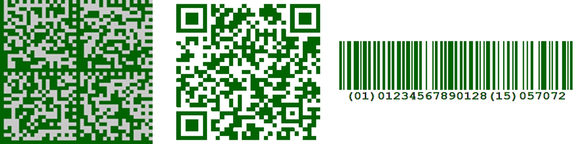
Digital printing enables flexible PCB identification and serialization
- Serialization codes in conjunction with solder mask printing
- Static and dynamic serialization with one or multiple codes per panel
- Many formats, including barcodes, QR and data matrix