Inkjet Soldermask printing
 Inkjet printing is an additive manufacturing technology applying functional materials for a variety of applications. These functional materials can have dielectric, conductive, adhesive, mechanical, optical or chemical properties, and are printed with pico-liter sized droplets from a digital file.
Its precise drop placement and accurate drop volumes make functional inkjet printing suited to printed electronics, displays, OLED, sensors, PCBs, semiconductor assembly, chemical machining, photovoltaics, life science and optics.
Inkjet printing can create fine features down to 20 micron and replace techniques such as lithography, screen printing, spray coating and dispensing. There is no more need for masks and screens, significantly saving material usage and enabling short product changeover times.
With a typical distance between the substrate and the inkjet head of just under 1 mm, inkjet is a non-contact deposition technology. So, there is no risk of damaging fragile substrates. Inkjet can also deposit on top of existing 3D topology and fill trenches and cavities, which is a challenge for traditional techniques like screen printing.
Benefits
- It is a selective coating technology: material is only deposited where required. This reduces material consumption and avoids the challenge of removing surplus solder mask material
- No risk of removing small solder dams between IC contacts
- Inkjet allows different surface finishes, layer thicknesses and materials. Finally, inkjet has the ability to accurately align and scale the print image to the board
- Inkjet has the ability to accurately align and scale the print image to the board
- Additive and cost-effective solder mask deposition, eliminating photo processes
- Environmentally friendly,
reducing waste and material usage - Additive and cost effective solder mask deposition
- Eliminating photo and development processes
- Digital process, higher flexibility
- Solder mask thickness variable between 5 – 100 µm
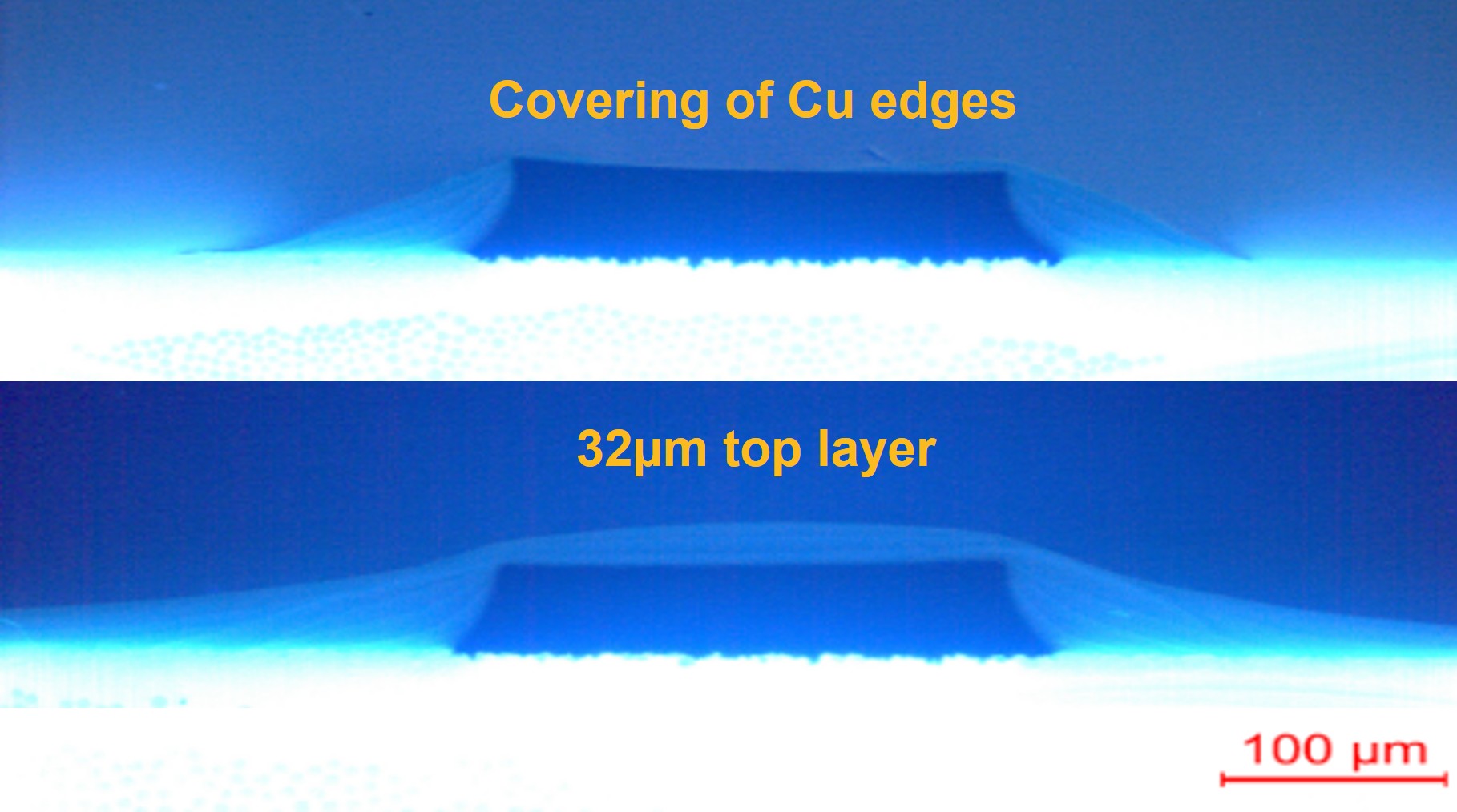
On copper and board material  Covering up to 120 µm copper thickness
Reliable solder mask thickness control at copper edges (4 µm and up)- Small feature sizes:
Line/space down to 75 µm in mass production
Via opening down to Ø 100 µm - Compatible with standard PCB pre-treatments
Acid cleaning, micro-etch, pumice, buff scrubbing
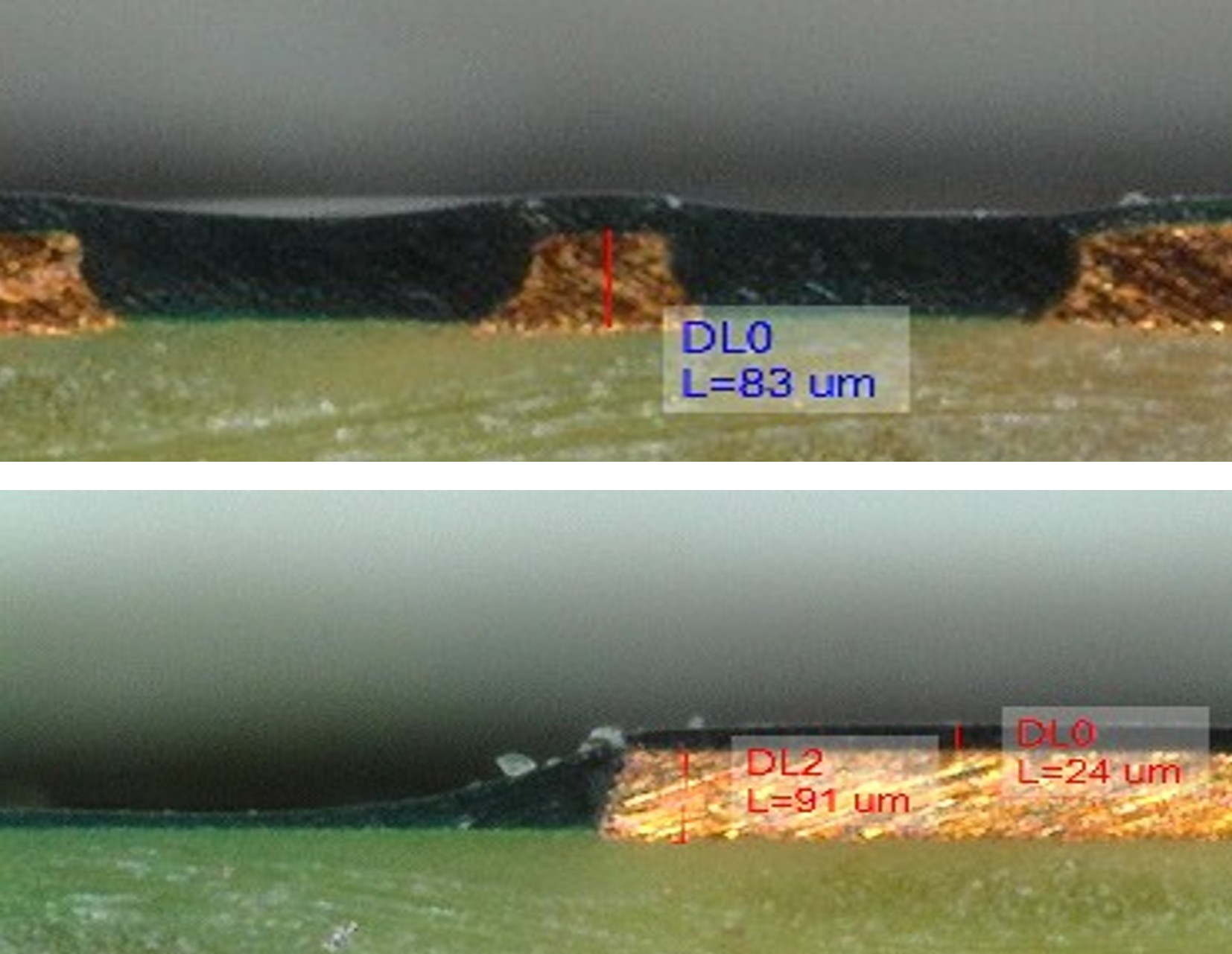
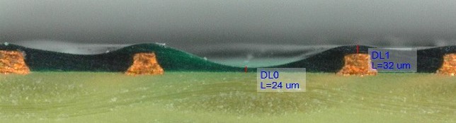
Multi-Layer Copper Edge Coverage
- Inkjet printing enables local deposition at the copper edges
- Enhanced solder mask thickness for better breakdown voltage
- Variable layer thickness for minimizing solder mask usage and optimal electrical performance